

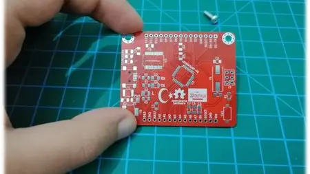
Arduino Nano Pcb Designs With Kicad

Arduino Nano Pcb Designs With Kicad
Published 6/2024
MP4 | Video: h264, 1920x1080 | Audio: AAC, 44.1 KHz
Language: English | Size: 3.71 GB | Duration: 4h 13m
Published 6/2024
MP4 | Video: h264, 1920x1080 | Audio: AAC, 44.1 KHz
Language: English | Size: 3.71 GB | Duration: 4h 13m
You will be able to design your own Arduino PCB using the KiCad program with this course.
What you'll learn
They will be able to design their own Arduino PCB cards and learn the logic of PCB card design.
KiCad
Gerber
2 Layer Design
Requirements
Basic knowledge of electronics is required.
Description
In this course, we are designing the Arduino Nano board.The KiCad program has been presented to us as a free program. Thanks to its easy and understandable interface, it makes designers comfortable to use.By following our course, you can learn a new program and contribute to your personal development.If you are tired of ready-made projects, if you want to design your own PCB board, this course is for you!Note: Our course has been prepared by using AI technology. KiCad is a constantly updated program. This course was shot with KiCad 5. In this course, you will be able to quickly learn prototyping without going into too much detail. The important thing is to understand the design logic. The interfaces do not change too much and you can easily adapt to new updates.About KiCadKiCad is an open source software suite for Electronic Design Automation (EDA). The programs handle Schematic Capture, and PCB Layout with Gerber output. The suite runs on Windows, Linux and macOS and is licensed under GNU GPL v3.Mission StatementThe goal of the KiCad project is to provide the best possible cross platform electronics design application for professional electronics designers. Every effort is made to hide the complexity of advanced design features so that KiCad remains approachable by new and inexperienced users, but when determining the direction of the project and the priority of new features, the needs of professional users take precedence.Project GovernanceThe KiCad project is governed by a technical committee made up of the members of the lead development team. Most decisions are made by a consensus of the technical committee. When a consensus cannot be reached the final decision is made by the project leader.HistoryKiCad was first released in 1992 by its original author, Jean-Pierre Charras. It has been in continual development since then and is now managed by the KiCad Development Team.The name of KiCad comes from the first letters of a company of Jean-Pierre Charras' friend "Ki" being combined with "Cad". But it now has no meaning other than being the name of the software suite. Mentioned by Jean-Pierre in an email.More KiCad history, general information, and advancements can be found in Wayne’s 2015, 2016, 2017, 2018, 2019, 2020, and 2021 FOSDEM presentations.
Overview
Section 1: Installation & Interface
Lecture 1 Introduction
Lecture 2 KiCad Installation 5.1.4_1. [Important]
Lecture 3 Important Reminder
Lecture 4 Quick Look at the KiCad Interface
Lecture 5 Page Settings
Lecture 6 Hot Keys
Section 2: Schematic Design
Lecture 7 FT232RL Symbol Design
Lecture 8 ATmega328P-AU Symbol Design
Lecture 9 5V Regulator
Lecture 10 ICSP
Lecture 11 USB
Lecture 12 ATmega328P-AU
Lecture 13 Pins
Lecture 14 Description Command
Lecture 15 Electrical Rules Check (ERC)
Lecture 16 Footprint Assignment
Section 3: PCB Design
Lecture 17 Component Placements
Lecture 18 Connection Tracks - 1
Lecture 19 Connection Tracks - 2
Lecture 20 Editing Connection Tracks
Lecture 21 Copper Plating
Lecture 22 Writing Operations
Lecture 23 Logo Placement
Lecture 24 Mounting Holes
Lecture 25 Logo - 1
Lecture 26 Logo - 2
Lecture 27 Board Color
Section 4: PCB Production
Lecture 28 How to Order Professional PCB?
Engineering students , teachers and anyone who wants to design their own card.